
Influence of Carrier Generation and Recombination on Memristivity
Jyoti Prasad Roy Choudhary1, *Barnali Pathak2
1B. H. College, Howly, Barpeta, Assam, 781316, India
2Assam Don Bosco University, Tepesia, Sonapur, Assam, 782402 ,India
* Corresponding address: barnalipathak11@gmail.com
Abstract
In this work, the influence of excess charge carrier generation and recombination processes in nanostructured materials is systematically incorporated to develop a theoretical framework for deriving the voltage–current (V–I) characteristics of a memristor. At the nanoscale, carrier dynamics play a crucial role in determining the electrical response of materials, and their contribution becomes particularly significant in devices exhibiting memory effects. By accounting for these excess carrier phenomena, the proposed approach provides a physically meaningful description of memristive behavior without relying exclusively on ionic migration mechanisms.
The resulting V–I characteristics obtained from this model exhibit a pinched hysteresis loop which is widely recognized as the defining fingerprint of memristive systems. The emergence of this characteristic loop confirms the validity of the proposed framework and demonstrates its ability to capture the essential features of memristor operation. Furthermore, the analysis indicates that memristivity can be understood as an intrinsic property arising from the fundamental carrier dynamics within nanostructured materials. Therefore, the present approach offers an alternative and potentially viable pathway for explaining the underlying physical origin of memristivity, particularly in nanostructures where conventional ion-based models may be insufficient.
Keywords: Memristor, Nanostructure Materials, Excess Charge Carriers, Pinched Hysteresis Loop
Introduction:
The memristor, first theoretically proposed by Leon Chua in 1971, represents a concept that has evolved over more than five decades of scientific inquiry [1], [2]. Despite its early theoretical foundation, the memristor remained largely unexplored experimentally until a major breakthrough was achieved in 2008, when convincing experimental evidence was demonstrated at Hewlett-Packard (HP) Laboratories [3]. This milestone sparked widespread interest and positioned the memristor as a fundamental circuit element alongside the resistor, capacitor, and inductor. Since then, memristors have been regarded as one of the most promising candidates for a wide range of future technological applications, including nonlinear analog circuit design, chaotic systems, non-volatile memory technologies, and neuromorphic computing architectures [4]. Consequently, memristor research has emerged as an active and rapidly expanding frontier in modern condensed matter physics and nanoelectronics.
With recent advancements in sophisticated fabrication and characterization techniques, remarkable progress has been made in the discovery and development of new memristive materials exhibiting enhanced switching performance, scalability, and reliability [5]. Alongside experimental advancements, there has been growing interest in understanding the underlying physical mechanisms responsible for memristive behavior and in establishing a robust theoretical framework capable of explaining experimental observations [6]. In the pursuit of a fundamental understanding of resistive switching phenomena, a wide variety of models and mechanisms have been proposed [6], [7]. The majority of these models attribute memristive switching to the movement and redistribution of ionic species, such as cations (Ag or Cu ions) and anions (oxygen ions or oxygen vacancies), which act as internal state variables controlling the resistance of the device.
In addition to ion-based mechanisms, several studies have reported resistive switching governed by purely electronic effects, where ionic motion plays a negligible or no role [8]. At the nanoscale, materials are known to exhibit unconventional and sometimes unexpected responses due to quantum confinement, enhanced surface effects, and strong electron interactions. Numerous experimental investigations have revealed that memory effects can arise in a wide range of nanostructured systems through different physical mechanisms, including phase transitions within the material, resistance modulation induced by thermal or electrical excitation of charge carriers, electrochemical filament formation, and spin-torque-driven processes [9]. These diverse observations highlight the necessity of identifying an appropriate and universal physical basis for memristivity, particularly in the nanoscale regime.
Importantly, memristive behavior has also been observed in pure metallic nanostructures where ionic migration or oxygen vacancy dynamics are absent [8]. This suggests that doped oxygen vacancies or mobile ions cannot be regarded as the sole contributors to the internal state variable responsible for memristive switching. In light of these findings, it becomes essential to explore alternative descriptions of the state variable that do not rely on doped ions and are therefore applicable to undoped or pure materials as well.
In this context, the present work considers an alternative switching mechanism in nanostructured memristors based on the generation and recombination of charge carriers. Specifically, we propose that various forms of internal agitation—such as electrical, thermal, or field-induced excitation—can lead to the generation of excess electrons and holes within the nanostructure. The increased population of charge carriers enhances the electrical conductivity of the system, resulting in a decrease in resistance. Conversely, when the excitation is reduced or removed, the excess electrons and holes gradually recombine and neutralize the voltage terminals, thereby restoring the resistance to its original state. This dynamic process of carrier generation and recombination gives rise to a history-dependent resistance, which is the defining characteristic of memristive behavior.
The concept of carrier-based switching has also been employed in earlier studies using different theoretical approaches, with varying degrees of success in explaining experimental results [7]. Building upon these prior efforts, the present paper incorporates the electron-hole generation and recombination mechanism into a mathematical formulation inspired by the formalism developed in [10]. Using this adapted framework, we derive the voltage–current (V–I) characteristics of a memristor governed by carrier dynamics.
The resulting model successfully reproduces the essential features of volatile memristive systems, including non-linear behavior and the characteristic pinched hysteresis loop in the V–I plane [11]. Through detailed analysis, we demonstrate that the proposed approach captures the fundamental signatures of memristivity and provides valuable physical insight into switching phenomena in nanostructured materials. This study suggests that carrier generation and recombination can serve as a viable and generalized physical basis for memristive behavior, offering an alternative theoretical perspective that is particularly relevant for pure and undoped nanoscale systems [12], [13].
Theory
Pinched hysteresis in the voltage-current relation is an important characteristic of memristor [1], [4]. In order to exhibit hysteresis behavior, the relationship between current i(t) and voltage v(t) must depend on internal state variable ξ(t) that represents the memory of the device. This state variable changes with time depending on the applied electrical signal and determines the instantaneous resistance (memristance) of the device. In order to have hysteresis, i(t) and v(t) relationship requires a state variable ξ(t), satisfying the following relation [4]
The dynamics of internal state variable is governed by a differential equation
Inspired by several reports, we consider the following simple analytic form of these relations
As discussed earlier, consider that excess-carrier generation and recombination is responsible for the switching mechanism in the nanostructure memristor. The creation of electrons and holes occurs due to different agitations inside the nanostructured memristor, such as electrical excitation and other internal disturbances. These generated charge carriers increase the number of free carriers available for conduction. As a result, the conductivity of the device increases and the resistance decreases. Thus, the presence of excess electrons and holes inside the memristor leads to a low resistance state. On the other hand, when these carriers move toward the voltage terminals, they gradually recombine with each other and neutralize. Due to this recombination process, the number of free charge carriers inside the device decreases, which causes the resistance to recover toward its higher value. Therefore, the switching behavior of the memristor is governed by the generation and recombination of excess carriers inside the nanostructure. In this paper, we assume that the resistance R(t) is directly proportional to carrier concentration Q(t) at a particular instant of time and consider the simplest possibility for describing this relationship.
With this assumption, we now proceed our calculations as mathematical replica to [10]. At constant Voltage Q(t) is constant and let it be defined by
Where we define h(V) such that h(0)=1, so that
It is evident that when voltage increases, carrier concentration increases i.e.
Again, as concentration increases, recombination rate increases and then charge carriers decreases, i.e., the rate of decrease of carrier concentration is directly related to carrier concentration at that instant.
We combine both the characteristics as follows:
We will treats is relation as our state equation. Above equation can be solved to have
where A is an integration constant.
Let us consider periodically changing voltage V(t) with period T applied to this memristor. The charge concentration Q will start changing but after a number of it will come to periodic steady state and Q(t) will cycle with the same period T. So, in a periodic steady state the solution is
If t = 0 then,
Which lead to have.
Which can be rearranged to have.
Thus the expression for current becomes
To obtain A, multiply by eT/τ
This is the general value of the integrating constant.
Let the steady state carrier concentration depend on voltage in a linear way
Where, φ is a parameter.
Let the voltage change harmonically,
Then,
Substitute into the integral (2)
Split the integral
Solving these integrals, A, we obtain the integration constant as
Therefore the charge changes at any instant during the cycle is
And hence the current through the memristor becomes
Results and Discussion
Using a simulation code developed in MATHEMATICA we have obtained the i(t)–v(t) characteristic curve for the memristor in accordance with eq.(2) and the corresponding results are shown in Fig 1. In this simulation, specific parameter values have been used in order to analyze the behavior of the device. The parameters chosen are V0=2 volts, Q0=100, α=20 and r = 8. Using these values, the response of the memristor has been studied for three different input signals having frequencies ω=2π, ω=4π, and ω=10π. These three cases are represented in the figure by dashed, dotted, and solid curves respectively. From the obtained V–I characteristic curves, we observe the presence of a pinched hysteresis loop, which is the most important characteristic feature of a memristor. The curves pass through the origin and form a looped structure when the applied voltage varies periodically with time. This behavior indicates that the current through the device depends not only on the instantaneous voltage but also on the previous state of the system. Furthermore, it is also observed that the area of the hysteresis loop decreases as the frequency of the applied voltage increases. For the lower frequency input signal, the loop is wider, while for higher frequency signals the loop becomes narrower. This behavior demonstrates another important property of memristors, namely that the hysteresis effect becomes weaker at higher frequencies of the applied voltage.
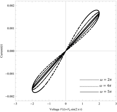
Fig.1. V-I Characteristics of a memristor.
Conclusion
We focus on excess carrier generation and recombination within nanostructures under an applied electric potential as the physical origin of memristive behavior. In a nanostructured memristor, the application of an external electric potential produces internal excitations that lead to the generation of excess charge carriers in the form of electrons and holes. These carriers increase the carrier population inside the nanostructure and contribute to electrical conduction through the device. The concentration of the excess carriers does not remain constant; rather, it changes continuously due to the simultaneous processes of generation and recombination. As electrons and holes are created, the number of free carriers increases, which modifies the conduction properties of the device. When these carriers recombine and neutralize each other, the carrier concentration decreases, leading to a recovery of the original conduction state. In this model, the resistive switching behavior of the memristor arises from these variations in the concentration of excess carriers within the nanostructure. To describe this behavior quantitatively, we use the mathematical formalism introduced in [10]. Based on this formalism, an expression is derived for the total charge stored in the device, which represents the amount of excess carriers present at a given instant of time. The obtained expression for the stored charge, the device current is subsequently calculated as a function of the applied voltage. The analysis leads to a current-voltage response that exhibits a pinched hysteresis loop, which is a fundamental characteristic of memristive systems. In addition, it is observed that the area enclosed by the hysteresis loop decreases as the excitation frequency increases, indicating that the hysteresis effect becomes weaker at higher frequencies. These features are well known characteristics of memristors [1], [4]. Since the combined framework of electron-hole pair generation and recombination, together with the methodology presented in [10], successfully reproduces the key signatures of memristive behavior, this approach can be considered as an alternative model for explaining memristive behavior in nanostructured devices.
References
- Chua, L. (1971). Memristor: The missing circuit element. IEEE Transactions on Circuit Theory, 18(5), 507-519. https://doi.org/10.1109/TCT.1971.1083337
- Jain, A., & Bilbault, J. M. (2022). Review on the basic circuit elements and memristor interpretation: Analysis, technology, and applications. Journal of Low Power Electronics and Applications, 12(3), 44. https://doi.org/10.3390/jlpea12030044
- Strukov, D. B., Snider, G. S., Stewart, D. R., & Williams, R. S. (2008). The missing memristor found. Nature, 453(7191), 80-83. https://doi.org/10.1038/nature06932
- Pershin, Y. V., & Di Ventra, M. (2011). Memory effects in complex materials and nanoscale systems. Advances in Physics, 60(2), 145-227. https://doi.org/10.1080/00018732.2010.544961
- Xiao, Y., Jiang, B., Zhang, Z., Ke, S., Jin, Y., Wen, X., & Ye, C. (2023). A review of memristor: material and structure design, device performance, application and prospects. Science and Technology of Advanced Materials, 24(1). https://doi.org/10.1080/14686996.2022.2162324
- Panda, D., Sahu, P., & Tseng, T. Y. (2018). A collective study on modeling and simulation of resistive random access memory. Nanoscale Research Letters, 13(8), 1-48. https://doi.org/10.1186/s11671-017-2419-8
- Vongehr, S. (2012). The missing memristor: Novel nanotechnology or rather a new case study for the philosophy and sociology of science? Advanced Science Letters, 17(1), 285-290. https://doi.org/10.1166/asl.2012.4241
- Johnson, S. L., Sundarajan, A., Hurley, D. P., & Strachan, D. R. (2010). Memristor switching of single-component metallic nanowires. Nanotechnology, 21(12), 125204. https://doi.org/10.1088/0957-4484/21/12/125204
- Caravelli, F. J., & Carbajal, J. P. (2018). Memristors for the curious outsiders. Technologies, 6(4), 118. https://doi.org/10.3390/technologies6040118
- Makarov, V. S., Misseis, A., & Chua, L. (2014). An analytical model of memristors in plants. Plant Signaling & Behavior, 9(10), e972887. https://doi.org/10.4161/15592324.2014.972887
- Wang, Y., Wang, W., Zhang, C., Kan, H., Yue, W., Pang, J., Gao, S., & Li, Y. (2022). A digital-analog integrated memristor based on a ZnO NPs/CuO NWs heterostructure for neuromorphic computing. ACS Applied Electronic Materials, 4(7), 3525-3534. https://doi.org/10.1021/acsaelm.2c00495
- Zhang, J., Du, J., Yang, C., Liang, H., Cao, Z., Duan, X., Yan, W., Zhao, Y., & Sun, B. (2024). Memristor-based electronic devices towards biomedical applications. Journal of Materials Chemistry C, 12(1), 50-59. https://doi.org/10.1039/D3TC03034B
- Thakkar, P., Gosai, J., Gogoi, H. J., & Solanki, A. (2024). From fundamentals to frontiers: a review of memristor mechanisms, modeling and emerging applications. Journal of Materials Chemistry C, 12(5), 1583-1608. https://doi.org/10.1039/D3TC03629H